Microelectronics & Semiconductor Wastewater Treatment - Nanostone Ceramic Membranes
Applications
Microelectronics / Semiconductor Wastewater Treatment
Advanced Ceramic Membrane Filtration for Microelectronics / Semiconductor Wastewater Treatment
Semiconductor fabs are facing increased scrutiny for their environmental impact, particularly as demand for chip design innovation intensifies.
As semiconductor technologies advance and feature sizes on chips get smaller, more processing or “mask layers” are required. Each additional mask layer increases water demand, significantly driving up the environmental footprint from a water perspective.
Fabs are often located in areas where they compete with municipalities for freshwater, frequently using tap water that is further treated to ultrapure water (UPW) standards. This escalating demand places a significant strain on existing freshwater supplies and can jeopardize operations as the industry rapidly expands to meet growing product demand. Hence, the importance of effective and efficient wastewater treatment for reuse continues to grow, ensuring sustainable water management and supporting the industry’s growth and innovation.
Semiconductor wastewater contains high concentrations of solids and abrasive particles, presenting significant treatment challenges:
- Grinding and Cutting Wastewater: Contains abrasive particles that can damage conventional membranes.
- CMP (Chemical Mechanical Planarization) Wastewater: Contains fine particulates and requires coagulation and pH adjustment before filtration.
- HF (Hydrofluoric Acid) Wastewater Reuse: Requires robust treatment to enable reuse and reduce environmental impact.
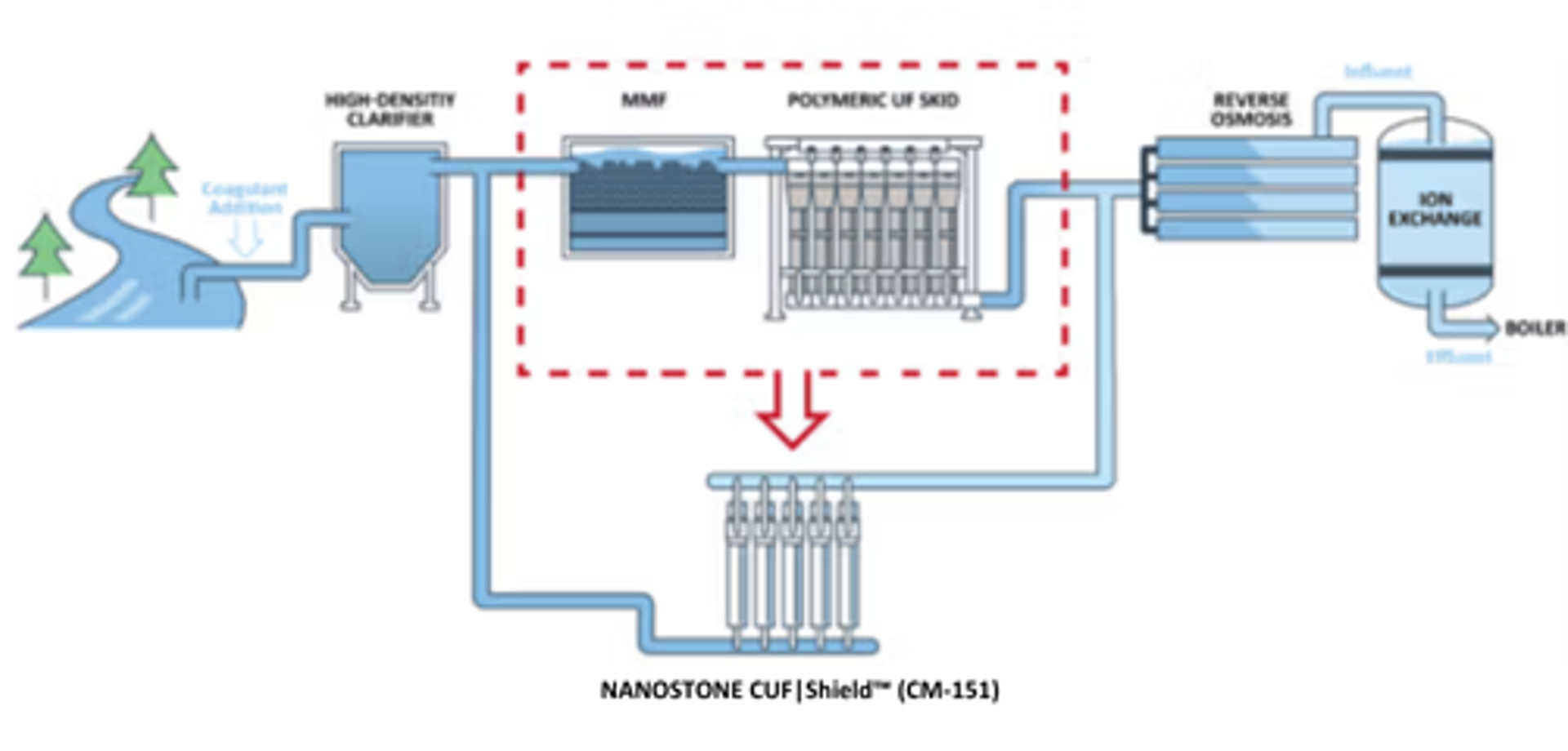
Our technology addresses these challenges by providing effective pretreatment for these wastewater streams, ensuring compliance with stringent environmental regulations and supporting water reuse initiatives. The Nanostone CUF|Shield™ (CM-151) ceramic ultrafiltration (UF) membrane system offers a smaller footprint, high resistance to abrasion, efficient backwash capability, and a high feed water solids limit, making it ideal for treating various wastewater streams in semiconductor plants.
Why Nanostone for Microelectronics / Semiconductor Wastewater Treatment
Approach & Benefits
Our Ceramic Ultrafiltration (CUF) Membranes enhances treatment efficiency by leveraging advanced filtration technology that directly addresses high turbidity and abrasive particles. Designed to streamline operations while meeting strict environmental regulations, our systems not only optimize water quality but also support sustainable reuse initiatives.
- Nanostone’s Solutions:
- Grinding and Cutting Wastewater: Direct filtration using the CUF|Shield™ (CM-151) membrane without any pretreatment.
- CMP Wastewater: Coagulation and pH adjustment followed by filtration with the CUF|Shield™ (CM-151) membrane.
- Unique Features:
- Streamlined Treatment: Simplifies the treatment process, reducing complexity and operational costs.
- High Feed Turbidity Tolerance: Can handle feed water with turbidity up to 10,000 NTU.
- Resistance to Abrasive Particles: Ensures longevity and reliability of the membrane.
- Nanostone’s solutions provide several benefits:
- Improved Water Quality: Ensures high-quality effluent suitable for reuse.
- Increased Efficiency: Simplifies the treatment process, reducing operational downtime and maintenance requirements.
- Reduced Footprint: Compact design fits into space-constrained facilities.
- Cost-Effectiveness: Lowers operational and capital expenses.
- Regulatory Compliance: Helps facilities meet stringent environmental regulations and achieve high water reuse rates (>90%).
Proven Success
Nanostone's Impact in Microelectronics
and Semiconductor Wastewater Treatment
North American Semiconductor Fabricator Case Study
- Challenge Overview:
The facility needed to upgrade its HF wastewater treatment to address compliance concerns and enable reuse. - Nanostone Solution:
Implemented the CUF|Shield™ (CM-151) UF membrane system, enabling wastewater reuse and reducing the need for fresh water. - Benefits Achieved:
- $800,000 in annual savings through reduced treatment costs, discharge fees, and freshwater acquisition.
- Reliable operation with a 95% recovery rate and minimal maintenance.
- Enhanced system stability and compliance with environmental regulations.
For more details, visit North American Semiconductor Fabricator project page.
Advanced Large-Scale Integration Assembly and Test Factory in Asia Case Study
- Challenge Overview: The facility faced declining treatment capacity and rising costs due to the fouling of polymeric UF membranes.
- Nanostone Solution: Replaced polymeric UF systems with CUF|Shield™ (CM-151) membranes, improving treatment capacity and operational stability.
- Benefits Achieved:
- Eliminated the need for third-party wastewater treatment.
- Achieved a recovery rate greater than 95%.
- Reduced maintenance and extended CIP cycles to over three months.
- Membrane life/robustness.
Sandisk SH Case Study

- Challenge Overview: The plant needed an improved treatment method for its high-turbidity mixed wastewater.
- Nanostone Solution: Replaced conventional treatment systems with the CUF|Shield™ (CM-151) ceramic UF membranes.
- Benefits Achieved:
- Achieved consistent water quality suitable for RO treatment.
- Reduced operational costs and footprint.
- Improved water recovery rates from 60% to over 80%.
Common Questions
About our Microelectronics / Semiconductor Application
How does Nanostone support the microelectronics and semiconductor industry?
How does Nanostone support the microelectronics and semiconductor industry?
Nanostone supports the semiconductor industry with advanced ceramic membrane technology that efficiently treats high-solids wastewater and promotes water reuse. Its compact, robust systems handle processes like grinding and CMP, ensuring high-quality effluent for ultrapure water while reducing pre-treatment steps and space requirements. This technology enhances sustainability, lowers costs, and helps facilities meet strict environmental regulations.
What contaminants can Nanostone’s technology remove in semiconductor wastewater?
What contaminants can Nanostone’s technology remove in semiconductor wastewater?
Nanostone’s technology effectively removes a wide range of contaminants from semiconductor wastewater, including abrasive particles from grinding and cutting processes, fine particulates from chemical mechanical planarization (CMP) wastewater, and other challenging contaminants. These ceramic membranes are specifically designed to handle high turbidity and abrasive solids, ensuring consistent effluent quality that is suitable for reuse in ultrapure water systems. The system provides reliable performance over time, even in demanding wastewater environments.
Sweetspot Applications
Explore Nanostone's Advanced Water Treatment Applications

Innovative Ceramic Membrane Solutions for Cleaner, More Sustainable Water
Nanostone's ceramic membranes enhance RO system performance by optimizing the pretreatment process. They efficiently remove suspended solids and pollutants, ensuring better water quality and reducing fouling risks. Ideal for both municipal and industrial applications, these membranes improve efficiency, sustainability, and cost-effectiveness in water treatment.
Book Your Discovery Call
Are you ready to transform your water treatment processes?
Book a free consultation with our experts to discuss your semiconductor wastewater treatment challenges and explore how Nanostone’s Ceramic Ultrafiltration technology can improve water reuse, operational reliability, and treatment efficiency. Fill out the form below to schedule your session.